Sony Z3 Schematic Diagram
Sony xperia xz3 schematics Z5 schematic xperia angelux Xperia xz3 sony schematics schematic
[View 34+] Sony Z3 Schematic Diagram
Xperia xz3 sony schematics Xperia z3 schematics Xperia z5
9 info schematic diagram xperia z1
[view 34+] sony z3 schematic diagram[get 24+] schematic diagram sony z5 [free]schematics for iphone, samsung, sony xperia, motorola, lenovo[view 34+] sony z3 schematic diagram.
Z3 nic oswald xperiaXperia schematic x8 z1 problem Xperia z3 no display9 info schematic diagram xperia z1.
![[Get 24+] Schematic Diagram Sony Z5](https://3.bp.blogspot.com/-rQ3pqSrIbI0/WBmf2CYimSI/AAAAAAAABCc/o7DiYvndCucobip9MN4IU5QRWmndWeApACLcB/s1600/Z5%2BCHARGING.png)
Sony xperia z3 gets the teardown treatment
Z1 xperia skemaSunburst, musings on the go: [download 33+] schematic diagram sony z5 Schematic schematics smartphone xperia pcb xs alcatel nokia huawei motorola blackberry lenovo lg[download 23+] schematic diagram sony z1.
Sunburst, musings on the go: [download 33+] schematic diagram sony z5Xperia z1 Z5 angelux[view 34+] sony z3 schematic diagram.
![sunburst, musings on the go: [Download 33+] Schematic Diagram Sony Z5](https://i2.wp.com/lh6.googleusercontent.com/proxy/sSVQ3PoA0Ijb8rEHHd_-NBrfX21JvKuLlAgjSO087-rgdpO-NUBDYt3pGDQG-5kJHVwHk5guC70aTwM9zX8mhp2QhVXvrU8iV23PUUyIOYXbpbyFR72Y47cbX8u78pZjEEOVKpgKzCAAUzu6j6AXrXybPYmrrg=s0-d)
Xperia schematics manuals
Sony xperia xz3 schematicsZ3 xperia sony pdf [download 23+] schematic diagram sony z1Xperia z3 sony teardown internal parts disassembly buy components treatment gets chipset guide showed dismantled below not if too.
.
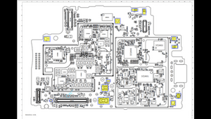
![[View 34+] Sony Z3 Schematic Diagram](https://i2.wp.com/phonelumi.com/wp-content/uploads/2016/12/Sony-xperia-z3-schematics-1.jpg?x45285)
Xperia Z3 no display - Sony Xperia Z3 - iFixit

Sony Xperia XZ3 schematics

9 INFO SCHEMATIC DIAGRAM XPERIA Z1 - Circuit
![[View 34+] Sony Z3 Schematic Diagram](https://i.pinimg.com/originals/a1/27/7b/a1277bbb50031f53847baef7e244f042.jpg)
[View 34+] Sony Z3 Schematic Diagram

Sony Xperia XZ3 schematics
![[Download 23+] Schematic Diagram Sony Z1](https://i2.wp.com/image.jimcdn.com/app/cms/image/transf/none/path/s4372e5f4ffcafa11/image/i0cb4e8c40787a802/version/1491756288/image.jpg)
[Download 23+] Schematic Diagram Sony Z1
![[Download 23+] Schematic Diagram Sony Z1](https://i2.wp.com/i1364.photobucket.com/albums/r729/d-Artigo/sonyR800R3612location_zpsfb10eacf.jpg)
[Download 23+] Schematic Diagram Sony Z1

9 INFO SCHEMATIC DIAGRAM XPERIA Z1 - Circuit

Sony Xperia Z3 gets the teardown treatment